ASIA ELECTRONICS INDUSTRYYOUR WINDOW TO SMART MANUFACTURING
Hitachi High-Tech Beefs up Wafer Inspection Systems
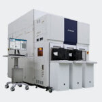
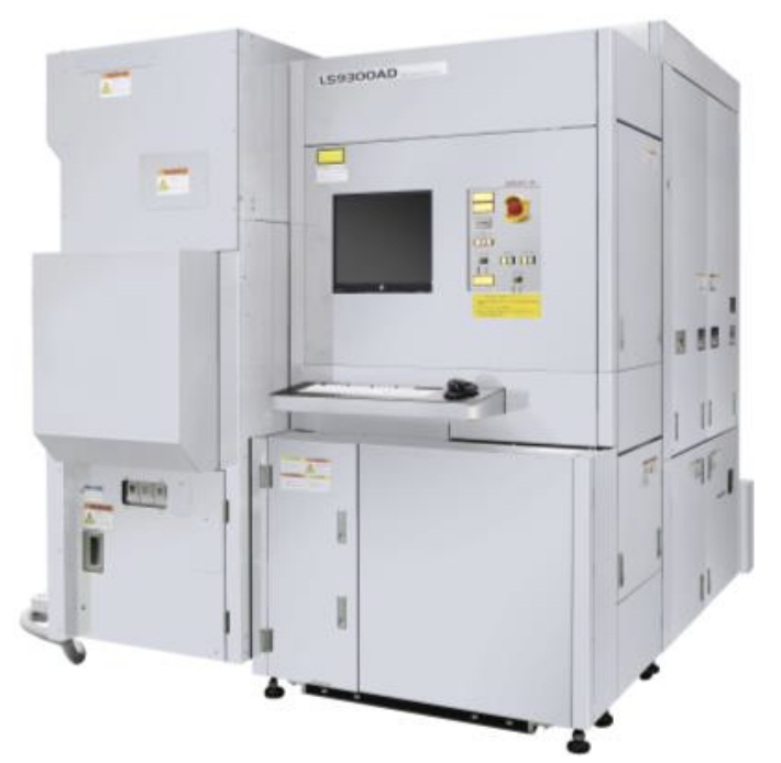
Hitachi High-Tech Corporation has launched LS9300AD for inspecting the front and backside of non-patterned wafer surfaces for particles and defects. In addition to the conventional dark-field laser scattering detection of foreign material and defects, LS9300AD is equipped with a new DIC (Differential Interference Contrast) inspection function. Specifically, it enables the detection of irregular defects, even shallow, low aspect*1 microscopic defects. Additionally, LS9300AD has the wafer edge grip method*2 and rotating stage currently used in conventional products. This enables front and backside wafer inspection.
With the introduction of LS9300AD, Hitachi High-Tech enables reduced inspection costs and improved yield for semiconductor wafers and semiconductor device manufacturers. Mainly, it provides high-sensitivity and high-throughput detection of low-aspect microscopic defects.
New Product Development Background
Inspection of non-patterned semiconductor wafers’ (before circuit pattern formation) surfaces and backside surfaces has been used in quality assurance during wafers shipment and acceptance. Also, it is employed for particles control in various semiconductor device manufacturing processes.
Specifically, semiconductor wafer manufacturers use it for quality control to inspect defects and particles that occur during the wafer manufacturing process. In recent years, semiconductor devices have become smaller and more complex. Thus, the size of defects and foreign matter that affect yield in the semiconductor device manufacturing process has become smaller. Due to this, the need for managing all types of defects is increasing. Among them are low-aspect microscopic defects on the surface and backside of wafers. Also, in response to changes in the social environment, semiconductor production will likely. To control inspection costs, high-sensitivity and high-throughput inspection equipment is required.
New Key Technologies
Specifically, LS9300AD features the conventional dark-field laser scattering. It has a new DIC optical system that enables both high-sensitivity, high-throughput inspection, and detection of low-aspect microscopic defects.
(1) Built-in DIC Optics
While a dark-field laser irradiates the wafer surface, two beams separated from the DIC laser irradiate two different points on the wafer surface. When there is a difference in height on the wafer surface between the two points irradiated by the DIC laser, the phase contrast of the differential interference signal generated from the difference creates a high-contrast image of wafer surface unevenness. As a result, it is possible to detect the height, area, and position information of low-aspect microscopic defects on the wafer surface. In the past, it was difficult to detect using previous techniques.
(2) New DIC-compatible Data Processing System
Along with the DIC optical system, a dark-field laser scattering optical system and a data processing system for defect information obtained through the DIC optical system are installed. This enables simultaneous output of dark-field laser scattering and inspection maps from the DIC optical system. Therefore, it enables high-sensitivity inspection, even of low-aspect defect data, while maintaining a high inspection speed.
Hitachi High-Tech offers LS9300AD, metrology systems using electron beam technology, and optical wafer inspection systems. Therefore, it can meet customers’ needs in processing, measurement, and inspection throughout the semiconductor manufacturing process. Hitachi High-Tech will continue to provide innovative and digitally enhanced solutions to its products for the upcoming technology challenges. Moreover, it will create new value together with customers, as well as contributing to cutting-edge manufacturing.
*1 Low-aspect: Generally, aspect ratio refers to the aspect ratio of a rectangle. In this release, “low-aspect” refers to irregularities on the surface and backside of the wafer, microscopic defects with an extremely small ratio of depth to width.
*2 Wafer edge grip method: A method in which the wafer is fixed only at the edge during inspection
-15 March 2024-
- Share: